|
This website is kept for archival purposes only and is no longer updated.
Facilities and Equipment
Existing Mirror Facilities
As a consequence of their vigorous foil mirror and multilayer development programs, the X-ray Astrophysics Branch at Goddard has amassed an impressive list of facilities and equipment, essential in the fabrication and testing of the various components. These include: An array of equipment specifically designed for precision shaping reflector substrates. Automated mandrel sputtering chambers used in the deposition of Au and Pt on mandrels. Automated multilayer deposition chamber and auxiliary equipment for multilayer deposition on mandrels. Clean rooms with automated sprayers, special vacuum chambers, ovens and other equipment used in surface replication. An experienced work force which has remained intact through the fabrication of the five ASTRO-E flight mirrors. A 50-m-long evacuated X-ray beam line for testing mirror segments. Reflectometers used to evaluate multilayers deposited on glass flats or foil reflectors. Horizontal and vertical optical beam lines along with corresponding benches for tuning and evaluating mirror segments or complete mirrors. An array of metrology equipment for shape and surface evaluation. including laser scanners, Phase Contrast, 2-d Wyko and Atomic Force microscopes.
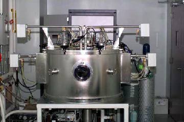
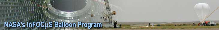
Fig. 1. GSFC high throughput automated multilayering facility.
The availability of such facilities along with the cumulative experience and expertise of several members of the mirror group greatly enhance our ability to design, fabricate and calibrate the InFOCmS mirrors. A similar capability for multilayering facilities is available at Nagoya.
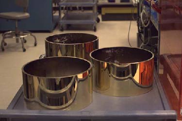
Fig. 2. Glass mandrels with deposited gold.
Existing Detector Facilities
The Detector Systems Branch has the necessary facilities to fabricate and test CdZnTe and CdTe detectors. The Detector Development Laboratory (DDL) is a 4000-square-foot, class 10 clean room with a large variety of semiconductor fabrication and testing tools. The fabrication tools include optical photolithography, chemical wet benches for etching, electroless deposition and cleaning, reactive ion etching, thin metal film vacuum deposition chambers (electron beam evaporation, thermal evaporation, sputterer), chemical vapor deposition systems (LPCVD - low presssure chemical vapor deposition; ECR - electron cyclotron resonance) and the deposition of insulators such as silicon oxide and silicon nitride, furnaces and ovens for oxidation, annealing, contact alloying, and curing of photoresist, a rapid thermal annealer, mechanical polishing, various optical inspection microscopes, and an ion implanter which can accelerate ions to 1 MeV. The testing tools include a probe station with cooling capabilities for electrical characterization of detectors (current-voltage, surface resistance, capacitance), an ellipsometer for characterization of dielectrics, and a stylus profiler for measurement of film thickness. Detectors can be integrated to electronics with the packaging facilities such as wire bonders and dicing saws in a clean room environment.
Fig. 3. Processing CZT in the GSFC cleanroom facility.
The Materials Engineering Branch has an extensive collection of tools to help carefully characterize the CdZnTe and CdTe materials we receive from various vendors. IR transmission and X-ray spectral mapping have been specifically developed to characterize and select large area CdZnTe and CdTe material for InFOCmS. Other valuable tools include Auger electron spectroscopy and X-ray photoelectron spectroscopy to measure the chemical composition of surfaces and thin films. A scanning electron microscope and X-ray analysis system can also be used to solve material and detector problems.
Arizona Facilities
The research group at the University of Arizona is investigating hybrid semiconductor detector arrays made of CdZnTe and CdTe for use as components of imaging systems for nuclear medicine under funding from the National Institutes of Health. Equiptment is available for testing semiconductor detectors under a wide range of operating conditions including at cryogenic temperatures. At Dr. Dereniaks' laboratory, a hybrid semiconductor array test facility is available for simultaneously testing up to 4 hybrids, and include a cooling chamber, PC based DSP data acquisition boards and data acquisition software operating in a LABVIEWTM enviornment. This system is designed to test hybrids using the 64x64 Arizona raster readout, but will be modified to handle hybrids using the InFOCmS readout. A Rucker and Kolls 660J wafer probe is also available, and an infrared transmission imaging system and gamma ray mapping system are under development. At Dr. Young’s laboratory at the University of Arizona Steward Observatory are wirebonders and a class 10,000 clean room containing a wafer spinner and mask aligner suitable for making detector arrays. We also have access to the CCD Laboratories of Dr. Michael Lesser at Steward Observatory in which are Research Devices M-8 and M-9 hybridization bonders. We recently demonstrated the capability to make hybrid detector arrays at this facility by hybridizing two 64x64 Arizona readouts together without the loss of any pixels. To round out the capability to make hybrids on campus, we will construct, with the assistance of Dr.s Young and Lesser, an indium evaporation system for making indium bumps on both CdZnTe detector arrays and readout wafers. This device will be housed in the Micro/Nano Fabrication Facility at the University of Arizona Optical Sciences Center, a 2000-square-foot facility containing class 100, 1000 and 5000 clean rooms. Additional equipment available in this facility include: a Carl Zeiss mask aligner, an ECR-RIE etching system, an electron beam lithography system, an electron beam metal evaporator and a Newport precision alignment packaging system. Facilities at the University of Arizona are available to the InFOCmS program and should be regarded as both complementary and as backups to those at NASA-GSFC.
InFOCmS Subsystems
In the existing program, we have procured or fabricated many important subsystems for the first flight. We have a housing for an 8-m focal length mirror. We have or have ordered forming mandrels, cutting fixtures, and replication mandrels for the mirror foils. The foils will be mostly fabricated by the end of this fiscal year and multilayering will be in progress. We have developed, fabricated and tested the carbon fiber truss for the flight telescope. We have built and tested the floating ball decoupler. We have procured 6 pieces of screened and tested CZT material for flight quality detectors. We have designed and fabricated a new sparse readout CTIA ASIC. We have fabricated 12 CZT and CdTe hybrids with the new ASIC. We have procured a CsI active shield with PMTs and readout electronics. We have arranged to use gyros, star cameras, magnetometers, sun sensor, and inclinometers for the pointing system. We have fabricated the pressure vessel for the detector focal plane and the optical bench for the mirrors. We have designed flight computer system and procured the hardware. Subsystems waiting for new funding are the decoupler support and launch constraint mechanism, momentum wheels, magnetic torquers, and the active alignment system. (These final systems will be designed and ready for procurement/fabrication by September.)
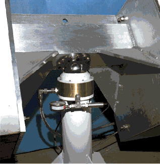
Fig. 4. Floating ball decoupler test.
|